Power ON/OFF Circuit Design for Nvidia Jetson Orin Nano
Issue Overview
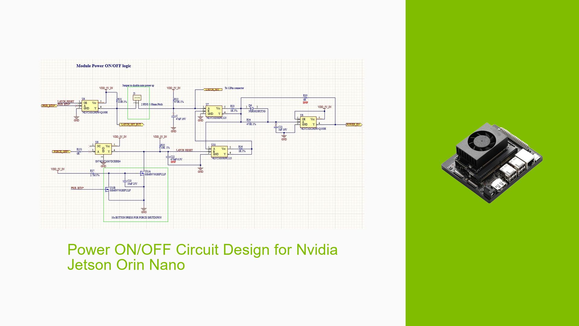
The main discussion revolves around the power ON/OFF circuit design for a custom carrier board for the Nvidia Jetson Orin Nano. The user has designed a carrier board based on the Jetson Nano reference design and the Migration document, as the Orin Nano dev kit was not available at the time. The key concerns are:
- The adequacy of using the Jetson Nano reference design for the power ON/OFF circuit
- The power-up sequence and its compliance with the Design Guide
- Powering the USB ports (VBUS) when only a single 5V input is available
- Potential issues with powering VBUS simultaneously with VDD_IN before the SYS_RESET signal is high
Possible Causes
-
Design Discrepancy: The latest Jetson Orin Nano reference design uses a different chip (EFM8SB10F2G) for the power ON/OFF circuit, which may lead to compatibility issues.
-
Power Sequencing: Incorrect power-up sequence could cause stability issues or prevent the board from functioning properly.
-
USB Power Management: Improper powering of USB ports might lead to power-related problems or USB functionality issues.
-
Single Power Input Limitation: Using only one power input (regulated 5V) instead of separate inputs for VDD_IN and USB power could potentially cause power distribution issues.
Troubleshooting Steps, Solutions & Fixes
-
Verify Power ON/OFF Circuit Design
- The existing design based on the Jetson Nano reference is considered adequate and should suffice for the Orin Nano.
- Ensure that the power-up sequence follows the Design Guide as shown in the provided image.
- Confirm that the 3.3V and 1.8V rails on the carrier are enabled by SYS_RESET.
-
USB Port Power Management
- For USB device ports:
- It’s acceptable to keep the same design as the P3449 schematic.
- For USB host ports:
- Refer to Figure 6-1 (USB Connection Example) in the Design Guide.
- Implement a load switch for proper power management.
- For USB device ports:
-
Single 5V Input Solution
- Short the DC 5V to VBUS, similar to the USB VBUS 5V supply only scenario on P3449.
- This approach addresses the concern of powering VBUS before the module is ready, which is not an issue in this case.
-
Power Sequencing Verification
- Double-check that the power-up sequence matches the following order:
- VDD_IN (5V)
- VDDQ_VDD_SYS (3.3V)
- VDD_1V8 (1.8V)
- SYS_RESET
- Use an oscilloscope to verify the timing of each power rail during startup.
- Double-check that the power-up sequence matches the following order:
-
USB VBUS Power Implementation
- Power the VBUS pins of the USB 2.0 connectors with the VDD_IN (5V) rail.
- This approach is acceptable and should not cause issues with powering VBUS simultaneously with VDD_IN before SYS_RESET is high.
-
Documentation and Testing
- Thoroughly document your final design choices and rationale.
- Perform comprehensive testing of the power system, including:
- Startup sequence verification
- USB functionality tests (both host and device modes)
- Stress testing under various load conditions
- Monitor power rails for stability and proper voltage levels during operation.
By following these steps and implementing the suggested solutions, you should be able to create a functional and reliable power system for your custom Jetson Orin Nano carrier board. Remember to always refer to the latest Nvidia documentation and guidelines for best practices and any updates to the design recommendations.
