Orin Nano: 3V3 I2C to 1V8 I2C Level Shifting Issues
Issue Overview
The discussion revolves around the challenges faced by users designing a custom carrier board for the Nvidia Jetson Orin Nano, specifically regarding the need to level shift I2C signals from 3.3V to 1.8V. Users have reported the following symptoms:
-
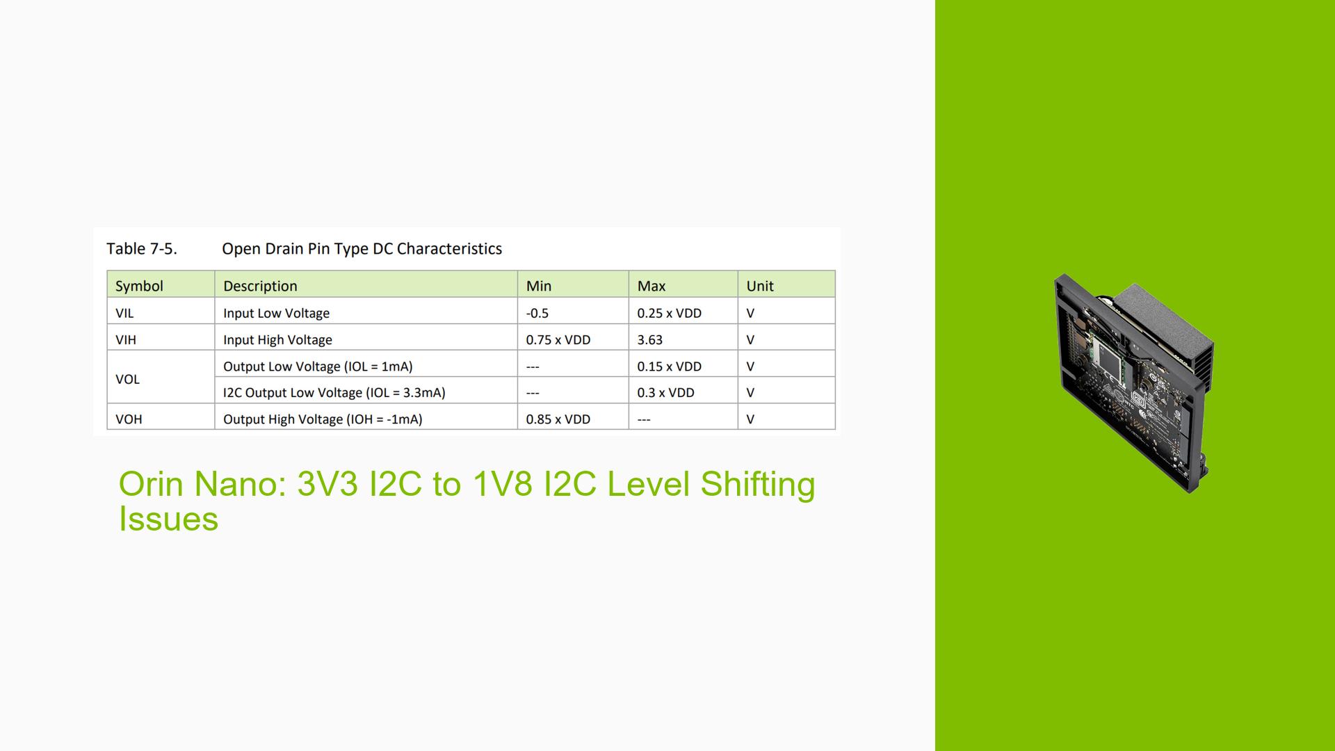
High VOL Levels: The maximum output low voltage (VOL) for I2C0 and I2C1 is specified as 0.3 * VDD, resulting in a VOL of 0.99V for the Orin Nano, which exceeds the acceptable threshold for many level shifters.
-
Level Shifter Incompatibility: The common level shifter ICs like TXS0102 have a maximum input low voltage (VIL) of 0.15V, making them unsuitable for use with the Orin Nano due to the high VOL.
-
Confusion Over Specifications: Users are questioning whether there is an error in the datasheet specifications for VOL, as it exceeds the I2C specification limit of 0.4V.
The issue primarily occurs during the design phase of custom hardware when attempting to integrate multiple I2C buses at different voltage levels. This has a significant impact on user experience, as it complicates hardware design and can lead to potential failures in communication between devices.
Possible Causes
-
Hardware Specifications: The datasheet specifies a high VOL for I2C outputs, which may not be compatible with standard level shifters.
-
Level Shifter Design Limitations: The architecture of common level shifters like FXMA2102 and TXS0102 may not accommodate the high VOL from the Orin Nano, leading to undefined states.
-
Misunderstanding of Voltage References: Users may misinterpret which voltage supply (internal or external) is being referenced in the datasheet, leading to confusion regarding compatibility.
-
Configuration Errors: Incorrect settings related to internal pull-up and pull-down resistors could affect the performance of I2C signals.
Troubleshooting Steps, Solutions & Fixes
-
Verify Datasheet Specifications:
- Ensure that you are referencing the most current version of the Jetson Orin Nano datasheet for accurate specifications regarding VOL and VIL.
-
Assess Level Shifter Compatibility:
- Check if using FXMA2102 or TXS0102 level shifters meets your design requirements based on their VIL specifications.
- Consider alternative level shifters that may have lower VIL thresholds suitable for your application.
-
Test with Different Configurations:
- Experiment with different pull-up resistor values on your I2C lines to see if adjusting these can bring VOL within acceptable limits.
- Use an oscilloscope or logic analyzer to monitor signal levels during operation.
-
Modify Internal Pull-Up/Down Settings:
- If applicable, tune internal pull-down resistor values to ensure that they meet I2C specifications.
- Review configuration settings related to drive strength; ensure they are set correctly for open-drain configurations.
-
Consult Additional Resources:
- Refer to application notes or design guides provided by Nvidia or other manufacturers regarding level shifting techniques.
- Engage with community forums or support channels for insights from other users who may have faced similar issues.
-
Consider Custom Solutions:
- If standard solutions fail, consider designing a custom level shifter circuit tailored to your specific voltage requirements and signal characteristics.
-
Documentation and Updates:
- Regularly check for updates on driver software or firmware that might address known issues with I2C communication on the Orin Nano.
- Keep documentation of any changes made during troubleshooting for future reference.
By following these steps, users can diagnose and potentially resolve issues related to I2C level shifting on the Jetson Orin Nano Dev board effectively.
