MIPI 4Lane 2.5G Instability Issue on Nvidia Jetson Orin Nano Dev Board
Issue Overview
Users are experiencing instability issues with the MIPI 4Lane configuration operating at 2.5G speed on custom carrier boards designed for the Nvidia Jetson Orin Nano SOM. The specific symptoms include:
- Frame drops and stream interruptions
- Some boards only work stably at lower speeds (2.3G/2.4G) for extended periods
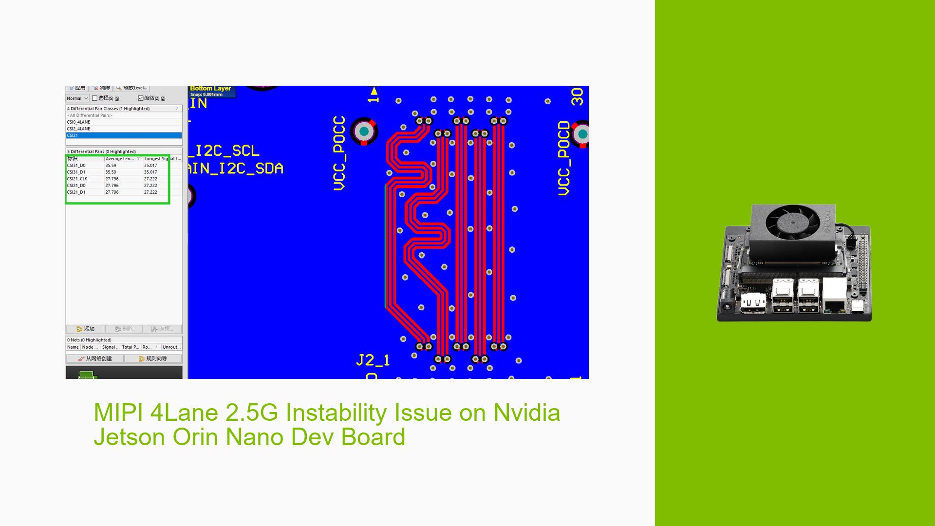
- The issue persists even with carefully designed adapter boards that control MIPI trace lengths and maintain equal length between differential pairs
The problem significantly impacts the functionality of the MIPI camera interface, limiting the ability to use the full 2.5G speed capability of the Orin Nano SOM.
Possible Causes
-
Signal Integrity Issues: The mismatch between CSI3_D0/D1 and CSI2_CLK signals may be causing instability at higher speeds.
-
PCB Layout Constraints: The SOM board’s connector pin arrangement, with CSI2_CLK/D0/D1 signals on the back and CSI3_CLK/D0/D1 on the front, could be contributing to signal timing discrepancies.
-
Inadequate Lane Matching: The 4-lane MIPI configuration (CSI2_CLK/D0/D1 + CSI3_D0/D1) may not be properly matched in terms of trace lengths on the SOM itself.
-
Timing Requirements: The strict timing requirement of maintaining data and clock signal time differences within 16ps at 2.5G operation may not be met due to layout constraints.
-
SOM Design Limitations: The Orin Nano SOM’s MIPI routing may not be optimized for 4-lane applications, potentially requiring compensation on the carrier board.
Troubleshooting Steps, Solutions & Fixes
-
Lane Configuration Testing:
- Test with 2-lane configurations (CSI2_CLK/D0/D1) and (CSI3_CLK/D0/D1) separately at 2.5G.
- If both 2-lane configurations work stably, focus on the interaction between CSI3_D0/D1 and CSI2_CLK.
-
Trace Length Adjustment:
- Implement a design with intentional length mismatch, making CSI3_D0/D1 traces approximately 8mm longer than CSI2_CLK/D0/D1.
- This approach has shown significant improvement, enabling stable 4-lane operation at 2.5G for over 24 hours on previously problematic boards.
-
Signal Integrity Analysis:
- Perform MIPI waveform tests near the SOM connector.
- Compare equal-length and unequal-length designs, looking for timing differences between lanes.
- The successful design showed a delay of about 50ps for the lengthened lanes compared to the unchanged lanes.
-
Reference Design Analysis:
- Examine the official carrier board reference design (P3768_A04.brd).
- Note that the J21 connector (supporting 1×2 lane or 1×4 lane CSI) also shows unequal trace lengths between CSI3_D0/D1 and CSI2_CLK/D0/D1.
- Calculate the theoretical delay differences and compare them to the 16ps guideline mentioned in the design guide.
-
Compensation Strategy:
- Consider implementing deliberate trace length mismatches on the carrier board to compensate for potential SOM-level routing discrepancies.
- Use the reference design as a starting point for determining appropriate compensation lengths.
-
Documentation and Support:
- Contact Nvidia support for clarification on the following points:
a. Whether the Orin Nano SOM’s MIPI routing is optimized for 4-lane applications.
b. If the 16ps timing requirement applies to the main chip or the SOM’s edge connector.
c. Confirmation of 2.5G 4-lane MIPI reception testing on the J21 connector of the reference design.
d. Explanation for the intentional length mismatch in the reference design.
e. Whether carrier boards need to implement unequal length designs to compensate for SOM routing.
f. Availability of documentation specifying exact compensation lengths for each MIPI lane relative to the clock.
- Contact Nvidia support for clarification on the following points:
-
Hardware Verification:
- Use high-speed oscilloscopes or signal integrity analyzers to verify MIPI signal quality and timing relationships.
- Pay special attention to the clock-to-data timing relationships across all lanes.
-
Temperature and Environmental Testing:
- Conduct extended stability tests under various temperature conditions to ensure the solution is robust across different operating environments.
-
Firmware and Driver Updates:
- Ensure that the latest firmware and drivers are installed on the Jetson Orin Nano.
- Check for any known issues or patches related to MIPI performance in the Jetson documentation or forums.
By following these steps and implementing the suggested fixes, users should be able to achieve stable 4-lane MIPI operation at 2.5G on their custom carrier boards for the Nvidia Jetson Orin Nano SOM. However, it’s crucial to work closely with Nvidia support for official guidance and to ensure that any modifications align with the platform’s design requirements.
