
CSI Camera Connector Limitations on Nvidia Jetson Orin Nano Dev Board
Issue Overview
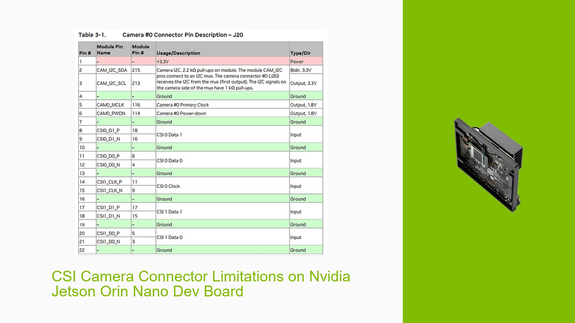
The Nvidia Jetson Orin Nano Development Kit has a limitation regarding the Camera Serial Interface (CSI) connector J20. Users are experiencing confusion about the purpose and functionality of certain CSI signals on this connector, specifically CSI0_D0_N/P and CSI0_D1_N/P. The main issue is that these signals cannot be used in either 2-lane or 4-lane mode due to the absence of CSI0_CLK_N/P on the J20 connector.
This limitation affects the camera interface capabilities of the development kit, potentially impacting users who require specific camera configurations or are designing custom solutions based on the Jetson Orin Nano platform.
Possible Causes
-
Hardware Design Limitation: The J20 connector on the development kit carrier board is designed to support only a 2-lane sensor configuration. This is due to the presence of CSI1_CLK instead of CSI0_CLK or CSI2_CLK, which are required for 4-lane configurations.
-
Software Constraints: The current software only supports 4-lane camera configurations with the lower clock lane of the 4-lane clock interface. This means that CSI0_CLK or CSI2_CLK are supported for 4-lane configurations, but not CSI1_CLK or CSI3_CLK.
-
Intentional Design Choice: The inclusion of CSI0_D0_N/P and CSI0_D1_N/P signals on the J20 connector might be intentional for future compatibility or custom designs, despite being currently unusable on the development kit.
Troubleshooting Steps, Solutions & Fixes
-
Understand the Limitations:
- Recognize that the J20 connector on the Jetson Orin Nano Dev Kit can only support a 2-lane sensor configuration.
- Be aware that CSI0_D0_N/P and CSI0_D1_N/P signals are currently unusable on the J20 connector of the development kit.
-
Use J21 for 4-Lane Camera Interfaces:
- If you require a 4-lane camera interface, use the J21 connector instead of J20.
- J21 uses CSI2_CLK and can support both 2-lane and 4-lane camera interfaces.
-
Custom Design Considerations:
- For custom designs not using the development kit carrier board, follow the guidelines in the Design Guide to support 4-lane mode.
- Implement the design using CSI0_CLK + CSI0_D0/1 + CSI1_D0/1 for 4-lane support in custom designs.
-
Device Tree Adaptation:
- When designing and adapting the device tree for custom camera modules, be aware of the available MIPI-CSI2 channels on J20.
- Ensure your device tree configuration matches the hardware capabilities of the J20 connector (2-lane mode only).
-
Software Limitations:
- Note that there are currently no plans to support 4-lane mode working with the higher clock lane (CSI1_CLK or CSI3_CLK).
- Keep track of software updates and release notes for any future changes in camera interface support.
-
Alternative Solutions:
- If you require 4-lane camera support and cannot use J21, consider exploring alternative Jetson modules or custom carrier board designs that meet your specific requirements.
-
Documentation and Support:
- Refer to the official Nvidia Jetson documentation for the most up-to-date information on hardware specifications and limitations.
- Consult the Nvidia Developer Forums or support channels for specific questions or clarifications regarding camera interface configurations.
By understanding these limitations and following the provided solutions, developers can effectively work within the constraints of the Jetson Orin Nano Dev Kit’s camera interface capabilities or make informed decisions about custom designs.