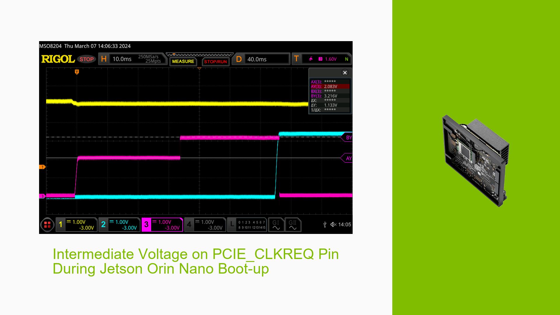
Intermediate Voltage on PCIE_CLKREQ Pin During Jetson Orin Nano Boot-up
Issue Overview
Users of the Nvidia Jetson Orin Nano Developer Kit are experiencing an unexpected intermediate voltage on the PCIE_CLKREQ pin during system boot-up. This issue occurs consistently and is observable even without any M.2 devices connected. The problem manifests as follows:
- An intermediate voltage of approximately 2.1V is observed on the PCIE_CLKREQ pin during power-on.
- The duration of this intermediate voltage state increases as the SoM (System on Module) heats up.
- In some cases, the voltage remains at ~2.1V and fails to reach the expected 3.3V level.
- This behavior is inconsistent with the expected high-Z state of the pin at power-on, as specified in the pinmux spreadsheet.
The issue impacts the proper functioning of PCIe devices and may lead to communication problems or device detection failures.
Possible Causes
-
Voltage tolerance enabling timing: The PCIE_CLKREQ pin is a 1.8V pin with 3.3V tolerance. The intermediate voltage may be caused by the timing difference between 1.8V and 3.3V power rails during boot-up.
-
Reverse leakage: There might be reverse leakage from the 3.3V pull-up resistor on the SoM to the 1.8V CMOS logic via the high-side FET body diode.
-
Thermal effects: The increasing duration of the intermediate voltage state with rising temperature suggests a potential thermal influence on the circuit behavior.
-
Pinmux configuration: Incorrect or suboptimal pinmux settings could contribute to the unusual voltage behavior.
-
Hardware defect: A manufacturing defect or component issue on the SoM could be causing the unexpected voltage levels.
Troubleshooting Steps, Solutions & Fixes
-
Verify pin configuration:
- Review the pinmux spreadsheet for the PCIE_CLKREQ pin.
- Ensure the pin is correctly configured as an open-drain bi-directional pin with an internal pull-up to 3.3V.
-
Test with different pinmux settings:
- Modify the pinmux configuration for PCIE1_CLKREQ using the pinmux spreadsheet.
- Try setting the pin as an input GPIO and observe any changes in behavior.
- Test the pin by setting it as "Output" and "Drive 0" to determine when the pinmux settings take effect.
-
Thermal analysis:
- Monitor the SoM temperature during boot-up and operation.
- Use thermal imaging or temperature sensors to identify any hotspots that might correlate with the voltage behavior.
- Ensure proper cooling and ventilation for the Jetson Orin Nano.
-
Voltage rail timing analysis:
- Use an oscilloscope to capture the power-up sequence of the 1.8V and 3.3V rails.
- Analyze the timing relationship between these rails and the PCIE_CLKREQ pin voltage.
-
Isolate the issue:
- Test the behavior on multiple Jetson Orin Nano units to determine if it’s a widespread issue or specific to one unit.
- If possible, test with a different carrier board to isolate whether the problem is in the SoM or the carrier board.
-
Check for firmware updates:
- Ensure you’re running the latest UEFI firmware version for the Jetson Orin Nano.
- Check for any available JetPack updates that might address this issue.
-
Consult Nvidia support:
- If the issue persists after trying the above steps, contact Nvidia developer support for further assistance.
- Provide detailed scope traces, thermal data, and pinmux configurations to help with diagnosis.
-
Workaround for affected systems:
- If the issue cannot be resolved, consider adding an external pull-up resistor to the PCIE_CLKREQ line on the carrier board to ensure it reaches the proper voltage level.
- Implement a delay in the boot process to allow the voltage to stabilize before initializing PCIe devices.
-
Hardware inspection:
- If possible, perform a visual inspection of the SoM, focusing on the area around the PCIE_CLKREQ pin for any signs of damage or manufacturing defects.
-
Documentation review:
- Thoroughly review the Jetson Orin Nano technical reference manual and application notes for any information on power sequencing or known issues related to PCIe signaling.
By systematically working through these steps, users should be able to either resolve the issue or gather sufficient data to escalate the problem to Nvidia for a more in-depth investigation.
